CONTENTS
| TO ORDER
3D Vertical NAND Flash Memory Technology, January 2015
(Roadmap, Product, Technology, Process, Design, Modeling, Test, Reliability)
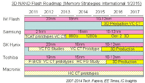
The first monolithic 3D IC's to make it into production are the 3D NAND flash
devices. The 30 billion dollar NAND Flash market targets systems using Solid
State Drives such as car navigation systems, industrial equipment, digital video
recorders. tablet computers, USB keys, and smart cards, as well as enterprise
and handheld computers. Early development of 3D NAND Flash began with Toshiba in
2007 with their bit cost scalable (BiCS) technology for vertical channel (VC)
change trapping (CT) NAND Flash and by Samsung with a series of technologies
culminating in 2009 in their terabit cell array transistor (TCAT) VC CT NAND
Flash. First into production was Samsung who announced in 2013 the inclusion in
their own SSD of a first generation 24-layer V-NAND device derived from their
earlier TCAT technology. Then in May of 2014 Samsung announced open production
of a larger 32 layer V-NAND. Toshiba has announced early production of their 3D
VC CT BiCS NAND Flash to begin in 2015 from an existing fab and full production
in 2016, if market conditions are favorable, from a new fab which is being built
for the 3D NAND flash. While early production is assumed to be of the 3D VC CT
BiCS device, they also had an interesting study in 2013 of a stacked horizontal
channel (HC) floating gate (FG) 3D NAND flash device. SK Hynix showed a series
of studies from 2011 to 2013 on 3D VC FG NAND Flash. They also did a study in
2014 of the relative benefits of charge trapping vs. floating gate 3D NAND
flash. In 2014 Hynix discussed a prototype of a VC CT gate-last device using
gate replacement. Macronix has produced a volume of technical papers on their 3D
horizontal channel/vertical gate HC CT NAND Flash as it has moved through
development. Their most recent test product is a 3D NAND flash in bit-alterable
technology and their most recent studies are on test, reliability and other
production issues but they have not announced a roadmap for production. Recently
Intel and Micron have indicated that a 3D VC CT NAND flash will be introduced in
the 2015 time frame. Meanwhile the planar NAND Flash devices continue in
intensive development. A full change from 2D to 3D NAND depends on the
cost-cross-over but the products are expected to co-exist for several years. A
tentative roadmap for 2D and 3D NAND Flash is shown in the following figure
where the 2D versions are in pink and the 3D versions in yellow. It can be
assumed that this is not the final version of this roadmap. 80+ pages.

DESCRIPTION | TO ORDER
3D Vertical NAND Flash Memory Technology
(Roadmap, Product, Technology, Process, Design, Modeling, Test, Reliability)
January 2015
Table of Contents
Executive Overview:
1.0 Overview and Roadmap of 3D Vertical NAND Flash
- 1.1 Roadmap of 3D Vertical NAND Flash
- 1.2 Overview of 3D Vertical NAND Flash
2.0 Vertical Channel Charge Trapping NAND Flash Technology
- 2.1 Overview of Vertical Channel Charge Trapping NAND Flash
- 2.2 Charge Trapping Bit Cost Scalable (BiCS) NAND Technology (Toshiba)
- 2.2.1 Wafer Fab for CT 3D Bit Cost Scalable (BiCS) Technology (Toshiba)
- 2.2.2 CT Bit Cost Scalable (BiCS) Technology for 3D Memory (Toshiba)
- 2.2.3 3D Stackable BiCS CT NAND Flash Memory (U. of Tokyo)
- 2.3 Charge Trapping 3D Vertical Channel NAND Technology (SK Hynix)
- 2.3.1 2nm Poly-Si Channel Junctionless FET TFT for 3D VC CT NAND (SK
Hynix)
- 2.4 Charge Trapping 3D Vertical Channel NAND Technology (Samsung)
- 2.4.1 Vertical CT V-NAND Production (Samsung)
- 2.4.2 3D Vertical Channel "a" Version 86Gb Vertical NAND Flash Chip
(Samsung)
- 2.4.3 3D Vertical Channel 128Gb NAND Flash (Samsung)
- 2.5 3D VC CT NAND Flash Overview (Intel, Micron)
- 2.6 Cost and Performance Trade-offs of 3D Vertical Channel CT NAND Flash
- 2.6.1 Overview of Cost and Performance Trade-offs of VC NAND Flash
- 2.6.2 Cost Analysis for the 3D VC NAND Flash (Schiltron)
- 2.6.3 Analysis of Cost and Reliability in Vertical Channel CT 3D
Flash(IMEC)
- 2.7 Materials and Process Development in 3D Vertical Channel CT NAND Flash
- 2.7.1 Overview of Materials and Process in 3D Vertical Channel NAND
Flash
- 2.7.2 Plasma Doping of High Aspect Ratio Structures in 3D Memory
(Varian/AMAT)
- 2.7.3 Trade-offs Between Macaroni and Full Channel 3D VC CT NAND Flash (IMEC)
- 2.7.4 Inspection Tool for Defects in 3D VC NAND Devices
(SK-Hynix, KLA-Tencor)
- 2.7.5 Material Challenges of 3D Memory Structures (Micron)
- 2.7.6 Charge Distribution in Thin HfO2 CT Layers in 3D Flash(Chinese
Academy of Sciences)
- 2.8 Design Considerations in 3D VC CT NAND Flash
- 2.8.1 Cell Current as a Function of Number of Layers in 3D VC NAND Flash
(Samsung)
3.0 Vertical Channel Floating Gate 3D NAND Flash
- 3.1 Vertical Channel Floating Gate 3D NAND Flash: DC-SF, MGCL (SK Hynix)
- 3.2 Metal Control Gate Last (MCGL) & Operation for DC-SF Cell
(Hiroshima U, SK Hynix)
4.0 3-D Horizontal-Channel/Vertical-Gate Charge Trapping NAND Flash
- 4.1 Overview of Vertical Gate CT NAND Flash
- 4.2 Vertical Gate BE-SONOS NAND Flash (Macronix)
- 4.2.1 Reducing Erase Saturation by Double-Trapping BE-SONOS CT NAND
(Macronix)
- 4.2.2 Reducing Vt Shift of SST and GST in 3D VG CT NAND (Macronix)
- 4.2.3 Dual-Channel 3D VG NAND Flash with Bit Alterable Characteristics
(Macronix)
- 4.2.4 3D p-channel VG CT NAND flash with BTBT Programming (Macronix)
- 4.2.5 3D VG BE-SONOS NAND Program and Read and Fail-Bit Detection
(Macronix)
- 4.2.6 Interference, Disturb, Programming Algorithms for MLC VG NAND
(Macronix)
- 4.2.7 Hot-Electron Assisted Programming in Split-Page 3D VG NAND Flash
(Macronix)
- 4.3 Process and Materials Issues in Vertical Gate CT 3D NAND Flash
- 4.3.1 Charge Loss Mechanism of Thin CT Layer at Variable Temperatures (CAS)
- 4.3.2 Shape Etching of Multi-Layer SiO2/Polysilicon for 3D NAND Flash
(Macronix)
- 4.4 Scaling VG 3D CT NAND Flash
- 4.4.1 Scaling VG 3D NAND by Thinning Poly-Si Channel and IPO (Macronix)
- 4.5 Process and Materials Effects of 3D VG NAND Flash
- 4.5.1 Antenna Protection Circuit for In-Process Charging Effects
(Macronix)
5.0 Horizontal Channel Floating Gate 3D NAND Flash
- 5.1 Overview of HC FG 3D NAND Flash
- 5.2 Horizontal Channel FG 3D NAND Flash (Toshiba)
6.0 Stacked Single Crystal Silicon NW (CSTAR) 3D NAND Flash Array
- 6.1 Overview of Stacked Single Crystal Silicon NW (CSTAR) NAND Flash Array
- 6.2 Layer Selection/Decode in Horizontal Channel CSTAR NAND Flash (Seoul Nat. U.)
- 6.3 3D Single Crystal Channel Stacked Array (CSTAR) NAND Flash (Samsung, Seoul Nat. U.)
7.0 Junctionless Nanowire for 3D CT Memory
- 7.1. Overview of Junction-less CT Nanowire Memories
- 7.2 Trench Junctionless Thin Body Poly-Si TFT Using Dry Etch for 3D (NTHU)
- 7.3 SiGE Buried Channel in Poly-Si NW CT Flash for 3D NV Memory Devices (NTHU)
- 7.4 Improved Erase speed in Junctionless HfO2/Si2N4 CT Flash Memories (NTHU)
- 7.5 Erase Constraint for 3D Junction-Less CT Memory Array
(P. di Milano, CNR Milano)
- 7.6 Gate-All-Around CT NW Memory with HfAlO trapping layer
(National Chiao Tung U.)
8.0 Reliability, Modeling and Test of 3D NAND Flash
- 8.1 Overview of Reliability and Test of 3D NAND Flash
- 8.2. Trap Analysis of V-NAND Cell using RTN Characteristics (Samsung)
- 8.3 Predictive Model of Channel Potential in GAA and DG 3D NAND Flash
(Samsung)
- 8.4 2D Model for 3D Retention Behavior in 3D CT NAND Flash (Peking U.)
- 8.5 Random Grain Boundary Trap Effects on Performance of 3D VG NAND
(Macronix)
- 8.6 Ibl Trap Effect in CT & FG Stacked NAND with Poly-Si body
(SK Hynix, SeoulNU)
- 8.7 Charge Pumping Signals in 3D Poly-Si Channel Devices (L.Johm Moores U,
IMEC)
- 8.8 Model of Random Grain Boundary Induced Variability in 3D NAND Flash (NCTU)
- 8.9 Programming Sequence Induced Back-Pattern Effect in 3D VG NAND
(Macronix)
- 8.10 Switching Traps in Vertical Poly-Si Channels (IMEC, KU
Leuven, L.J.Moores U)
- 8.11 Software Method of Disturb Alleviation for 3D Flash Memory (Macronix)
- 8.12 Modeling of Program Disturbance of 3D VC NAND Flash (SK Hynix)
- 8.13 Program Disturb Characteristics of 3D Vertical NAND Flash (Hynix)
- 8.14 Random Telegraph Noise in 3D Stacked NW Flash Memories (NCTU)
- 8.15 Comparison of 2D and 3D NAND (Micron Technology)
- 8.16 Retention Studies in 3D Vertical Channel Flash Devices (Tsinghua Univ, IMEC)
9.0 Design of Systems Using 3D VC NAND Flash
- 9.1 Reliability Enhanced Address Mapping for 3D NAND (HongKongPolyTech U, D.O.D. UofCalif)
- 9.2 Workload-Aware Design of 3D NAND Flash for Enterprise SSDs (Chuo U., U.Tokyo)
Bibliography
DESCRIPTION | CONTENTS
 To order "3D Vertical NAND Flash Memory Technology:


(Roadmap, Product, Technology, Process, Design, Modeling, Test, Reliability),
January 2015
Contact
Memory Strategies or
Send us the information requested below by e-mail, fax, or post along
with your check,
bank transfer, or purchase order for $975. ($850
if a Memory Technology Report has been ordered from Memory Strategies in the
past year.)
ORDER FORM:
Please send ______ copies of "3D Vertical NAND Flash
Memory Technology, January 2015" to:
| Name: |
Email: |
| Fax: |
Phone: |
| Company: |
| Address: |
| |
| |
| |
| Comments, Payment Information, etc.:
|
Report Format
____ PDF. Will be sent by email. Please send your order by email, if possible.
Printing hardcopy from PDF is permitted.
Submit Order and Payment
Information via:
Email:
info@memorystrategies.com, or
Fax: +1 512 900 2846
Post:
Memory Strategies International,
16900 Stockton Drive,
Leander, Texas 78641, U.S.A.
To pay
by:
- Credit Card: please fax credit card information to +1 512 900 2846
- Bank Transfer:
please send in your order and request
transfer details.
- Purchase Order: submit
purchase order details with order.
For more information, please Contact
Memory Strategies
| Home | Reports
| Seminars | Consulting
| Contact Us | About Us
|
Memory Strategies International, 16900 Stockton Drive, Leander, TX, USA,
78641; 512.260.8226 (phone), 512.900.2846 (fax). Send questions or
comments about this website to webmaster@memorystrategies.com.
Copyright © 2015 Memory Strategies International. All rights reserved. Legal stuff. Last Modified:
June, 2015.
